This is an old revision of the document!
Table of Contents
General registers
| Address | Desc. |
|---|---|
| 0xF0000000 | Hardware ID |
| 0xF0000004 | Soft reset |
| 0xF0000008 | Hardware setup |
| 0xF000000C | PLL - input clock divider |
| 0xF0000010 | PLL - clock multiplier |
| 0xF0000014 | PLL - primary clock divider |
| 0xF0000018 | PLL - secondary clock 1 divider |
| 0xF000001C | PLL - secondary clock 2 divider |
| 0xF0000020 | PLL - secondary clock 3 divider |
| 0xF0000024 | PLL - feedback frequency related |
| 0xF0000028 | PLL - feedback frequency related |
| 0xF000002C | PLL - feedback frequency related |
| 0xF0000030 | ?? |
| 0xF0000034 | Clocks - Pixel clock setting |
| 0xF0000038 | Clocks - Camera clock setting |
| 0xF000003C | Clocks - Audio amplifier clock setting |
| 0xF0000040 | Clocks - Clock setting for ?? (I2C0?) |
| 0xF0000044 | Clocks - Clock setting for ?? (I2C1?) |
| 0xF0000048 | Clocks - Clock setting for ?? (I2C2?) |
| 0xF000004C | Clocks - I2C3 clock setting |
| 0xF0000050 | Clocks - Clock setting for ?? (I2C4?) |
| 0xF0000054 | Clocks - SDIO clock setting |
| 0xF0000058 | Hardware reset |
| 0xF0000060 | ?? |
| 0xF0000064 | ?? |
Hardware ID
0xF0000000
This register serves to identify different hardware variations. Not sure if such variations occur in retail gamepads or if they are solely prototype stuff.
Regardless, the stock firmware checks different parts of this register before accessing certain hardware. A prominent example is I2C, for which there are two possible controllers from different vendors.
As far as I've seen, this register reads as 0x00041040 on production motherboards, both revisions 01 and 20.
| Bits | Desc. |
|---|---|
| 0-7 | Chip version (Type of GPIO, I2C and other stuff)0x10 (TS) 0x20 (ES1) 0x30 (ES2) 0x40 (ES3) 0x41 (MS01) |
| 8-15 | ?? |
| 16 | DRC base clock; 0=16MHz, 1=24MHz |
| 17-18 | ? |
| 19 | Type of PLL? |
The stock firmware checks bits 0-7 for value 0x41, and in that case:
- The I2C controller is different (Samsung instead of Renesas)
- In GPIO registers, bits 14 and 15 are swapped
- There are also differences in the video decoder and LCD controller
- There may be other differences too
Bits 16 and 19 are checked during hardware initialization, to choose the correct PLL settings.
Bit 16 seems to denote different hardware, additionally to the different base clock:
- when it is set, the bootloader doesn't interact with the UIC at all (otherwise it sends the 0x7F sync command and retrieves the UIC state if possible)
- Flash layout is also different, with firmware bank 2 being at 0x480000 instead of 0x500000
Reset registers
0xF0000004
Soft reset register. Setting bit 0 to 0 then 1 resets the CPU after a short delay.
0xF0000058
| Bits | Desc. |
|---|---|
| 0 | Reset IRQ controller |
| 1 | Reset timers |
| 2 | Reset RAM??? (displays static pattern) |
| 3 | Reset DMA |
| 4 | Reset SPI |
| 5 | ?? |
| 6 | Reset SDIO |
| 7 | Reset UART0 |
| 8 | Reset UART1 |
| 9 | Reset UART2 |
| 10 | Reset I2C0 |
| 11 | Reset I2C1 |
| 12 | Reset I2C2 |
| 13 | Reset I2C3 |
| 14 | Reset I2C4 |
| 15 | Reset audio controller |
| 16 | ?? |
| 17 | ?? |
| 18 | ?? |
| 19 | ?? |
| 20 | ?? |
| 21 | Reset LCD controller |
Setting a bit to 1 then 0 resets the corresponding hardware component. This register is 22 bits wide.
PLL
The gamepad starts at a clock of 16 MHz. PLL settings applied by the second stage bootloader change the system clock to 108 MHz.
Different settings are applied based on the base clock - it appears that some prototype versions use a base clock of 24 MHz.
| Setting | 16 MHz value | 24 MHz value |
|---|---|---|
| 0xF000000C | 13 | 20 |
| 0xF0000010 | 0x5E8000 | |
| 0xF0000014 | 5 | |
| 0xF0000018 | 510 | |
| 0xF000001C | 108 | |
| 0xF0000020 | 510 | |
| 0xF0000024 | 0xBC | |
| 0xF0000028 | 0x24 | |
| 0xF000002C | 0x3A1 | |
TODO: not known yet how the control registers work, ie. how to actually apply PLL settings
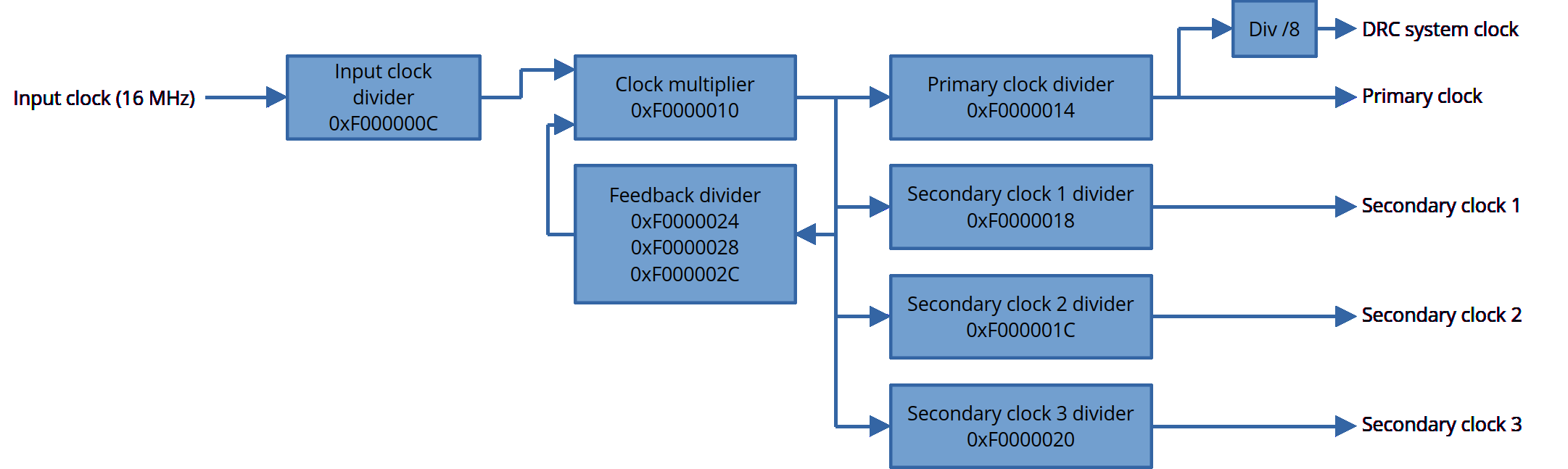
The base clock is divided by the input clock divider, then multiplied by the clock multiplier, producing a VCO frequency of 1728 MHz.
This frequency is then fed into 4 separate dividers to produce the primary clock and 3 secondary clocks. The primary clock is then divided by 8 to produce the DRC system clock.
The feedback frequency generation is not completely understood yet.
0xF000000C
Input clock divider. This register is 6 bits wide.
This seems to be a count-up divider, ie. setting it to 13 divides the input clock by 14.
0xF0000010
Clock multiplier. This register is 26 bits wide.
Bits 0-11 seem to be the fractional part of the multiplier.
0xF0000014
Primary clock divider. This register is 9 bits wide.
Possible values:
| Value | Divider |
|---|---|
| 0b0'0000'0000 | 4 |
| 0b0'0000'0010 | 4 |
| 0bx'xxxx'xxx0 | Register value |
| 0b0'xxxx'xxx1 | 2 |
| 0b1'xxxx'xxx1 | 2.5 |
This is a weird kind of divider: if bit 0 is set, the input is divided by 2 or 2.5 (depending on bit 8), but if bit 0 is cleared, the input is divided by the register value. Values 0 and 2 behave the same as 4.
It also appears that 2.5 isn't supported for the primary clock, and acts the same as 2?
0xF0000018
Secondary clock 1 divider. Function same as 0xF0000014.
0xF000001C
Secondary clock 2 divider. Function same as 0xF0000014.
0xF0000020
Secondary clock 3 divider. Function same as 0xF0000014.
0xF0000024
This register is related to the feedback frequency generation. This register is 12 bits wide.
0xF0000028
This register is related to the feedback frequency generation. This register is 12 bits wide.
Needs to be set to a nonzero value.
0xF000002C
This register is related to the feedback frequency generation. This register is 26 bits wide.
This register is related to 0xF0000028 in that one unit of 0xF0000028 equals 512 units of 0xF000002C.
Per-module clock settings
From 0xF0000034 to 0xF0000054
| Bits | Desc. |
|---|---|
| 0-7 | Clock divider |
| 8-10 | Clock source |
Clock source is one of 8 possible source clocks. Clock divider is a simple count-up divider, ie. setting it to 31 divides the selected clock by 32.
The following clock sources are available:
| Source | Default frequency | Description |
|---|---|---|
| 0 | 32 MHz | Always 32 MHz, likely just crystal X1 output |
| 1 | 12 MHz | Camera clock (from 0xF0000038) |
| 2 | ??? | ??? |
| 3 | 3.08 MHz | Audio bit clock (from audio amplifier) |
| 4 | 864 MHz | Primary clock |
| 5 | 3.38 MHz | Secondary clock 1 |
| 6 | 16 MHz | Secondary clock 2 |
| 7 | 3.38 MHz | Secondary clock 3 |
Peripherals may then divide their incoming clocks further. For example, in the case of I2C, the clock is divided by 24 before being output to the SCL line.
The fact that the camera clock can be selected as a clock source means it is possible to source the camera clock from itself. In practice, this doesn't collapse space-time or anything fun. It's more like plugging a power strip into itself.
Source 3 only works if the audio amplifier has been properly initialized.
Source 2 probably comes from another peripheral that needs to be initialized, not yet known which.